
Intel’s 18A Process Node: Whether the Company’s Foundry Reset Can Actually Threaten TSMC
Intel began risk production of its 18A process node in Q1 2026 — a milestone Intel’s leadership called “the most significant technical achievement in the company’s modern history.” 18A is Intel’s gate-all-around (GAA) transistor implementation, competing directly against TSMC’s N2 node on density and power efficiency. If 18A delivers on its specifications, Intel Foundry Services has a credible leading-edge logic product for the first time in a decade. If it does not, the foundry strategy Intel has staked approximately $45 billion in capital on over the past four years will face terminal questions from its investors and its customers.
The technical data published so far suggests Intel’s claims are partially supported and partially aspirational — which, at this stage of the risk production cycle, is better than the foundry strategy’s history since 2021 warrants.
18A Technical Specifications Against TSMC N2
Intel’s published 18A specifications claim approximately 10% performance improvement and 30% power reduction versus Intel 3 (its previous generation), at a transistor density comparable to TSMC N3E. Against TSMC’s N2 — which Intel is directly positioning 18A to compete with — the published claim is performance parity at comparable power, with Intel arguing a cost advantage from its RibbonFET (GAA) implementation and its integrated backside power delivery (PowerVia).
Independent foundry analysis from SemiAnalysis — the most technically rigorous public semiconductor analysis available — assessed 18A as capable of competing with TSMC N3E but not yet definitively at N2 parity. The integrated backside power delivery is genuinely novel and delivers meaningful power efficiency improvement; the RibbonFET implementation is technically comparable to TSMC’s GAA but is a first-generation production implementation that will require yield learning before it matches TSMC’s production maturity.
Yield is the operative variable. TSMC’s N2 has been in risk production since late 2025 with customer tape-outs; Intel’s 18A is in risk production now, approximately six months behind. At risk production, both nodes are operating below commercial yield — the percentage of functional chips per wafer that makes production economically viable. TSMC’s typical ramp from risk to commercial yield takes 12-18 months. Intel’s recent history (delays and yield problems on Intel 4 and Intel 3) makes the same timeline optimistic, but Intel’s manufacturing organisation has been substantially restructured under Pat Gelsinger and his successor, and the current 18A execution has proceeded more closely to schedule than its predecessors.
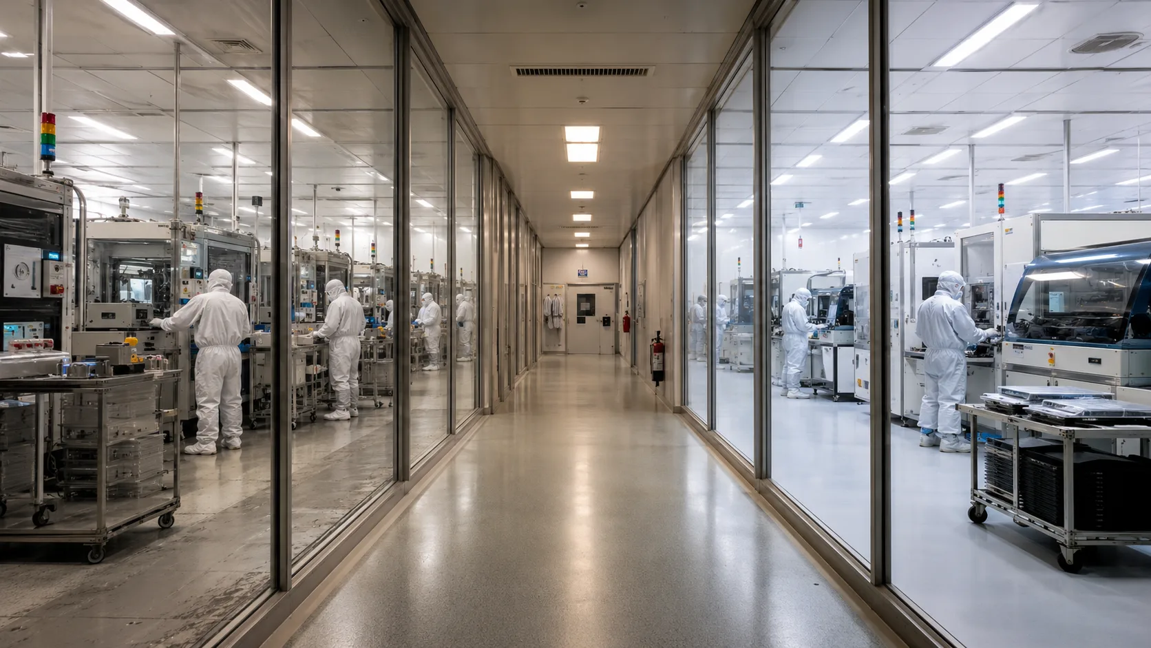
The IFS Customer Pipeline
Intel Foundry Services’ commercial viability depends on attracting customers who will commit multi-year wafer agreements at volumes that utilise Intel’s fab capacity. The current 18A customer pipeline includes Microsoft (confirmed via public disclosure), a US Department of Defense programme, and several undisclosed customers that Intel has characterised as “hyperscale and defence.”
Microsoft’s 18A commitment is the most commercially significant disclosed agreement. Microsoft has announced plans to use Intel 18A for undisclosed chip designs — likely custom AI accelerators for Azure rather than x86 consumer products — with wafer production scheduled to begin as 18A ramps to commercial yield in 2027. The Microsoft commitment represents a validation from a hyperscaler that has the engineering resources to evaluate foundry alternatives rigorously and the financial credibility to make the commitment meaningful.
The Apple relationship, which Intel and Apple have discussed publicly, remains uncertain. Intel’s Apple chip talks have centred on whether Apple would use Intel Foundry for future A-series or M-series silicon production alongside TSMC, providing geographic diversification for Apple’s most critical chip production. Apple has not committed publicly, and the timeline for any Apple IFS production would be 2028 at earliest given Apple’s multi-year chip design lead times. But a disclosed Apple commitment would be transformative for IFS’s commercial credibility in a way that even the Microsoft deal is not — Apple’s chip volumes are the single largest leading-edge logic customer in the world.
Intel’s Financial Position Under the Foundry Bet
Intel’s capital investment in its manufacturing turnaround has been the largest in US semiconductor history: approximately $20 billion in 2024 capital expenditure, $18 billion planned for 2025, and $14 billion in 2026 as the fab buildout matures and operating costs stabilise. The CHIPS Act provided approximately $8.5 billion in direct funding and approximately $11 billion in loan guarantees, reducing the net capital burden — but Intel is still running at negative free cash flow as the foundry investment scales ahead of revenue.
Intel’s Q1 2026 financial results showed IFS revenue of approximately $4.7 billion — up 8% year-over-year but still substantially below the $20 billion annual IFS revenue target that management has set for 2030. The gap between current IFS revenue and the target requires signing major external customers (currently, IFS revenue is dominated by Intel’s own product designs). At current external customer win rates, the 2030 target requires signing 3-4 major hyperscaler or fabless chip customer relationships within the next 18 months — a timeline that aligns with 18A reaching commercial yield and customer tape-out volumes.
What the Terafab Discussion Signals
The announced discussions about a potential Terafab programme — a large-scale US semiconductor manufacturing joint venture involving Intel, US government funding, and potentially industry partners including Elon Musk’s xAI — adds a geopolitical dimension to Intel’s foundry trajectory. The programme, which has not moved beyond discussion and MOU stages, would potentially provide additional capital for fab expansion at a scale that Intel could not fund independently.
The Terafab concept is driven by the same national security logic as the CHIPS Act: the US government wants leading-edge logic production capacity on American soil that is not dependent on TSMC’s Taiwan concentration. Intel is the only American company with the engineering capability to attempt this. Whether Terafab actually forms and at what terms are unknowns, but the discussion itself signals that Intel’s political capital with the US government remains intact — a non-trivial asset in the current semiconductor policy environment.
The Honest Assessment
Intel’s 18A represents the company’s most credible foundry technology since 2016. The GAA implementation is technically sound, the backside power delivery is genuinely innovative, and the execution to date has been closer to schedule than any of Intel’s prior leading-edge node programs since Cannon Lake. These are real improvements.
Against this is the context: TSMC’s N2 had its first 18 months of capacity pre-sold before production started, its CoWoS advanced packaging capacity is being doubled, and its gross margins are at 53%. TSMC’s existing customer relationships, production maturity, and supply chain ecosystem represent a structural moat that Intel cannot close through process node parity alone — it requires convincing customers to adopt Intel’s foundry infrastructure, which means qualification cycles, co-investment in packaging development, and management bandwidth commitments that customers will not make without a compelling risk-adjusted case.
The 2027-2028 window — when 18A reaches commercial yield, the first external customer chips begin production, and the Microsoft tape-out results become evaluable — will provide the definitive answer to whether Intel’s foundry reset produces a real competitor to TSMC or a perpetually-promising-but-second-tier alternative. The bet Intel’s investors have made is on the former. The semiconductor industry’s history of the past decade suggests caution about that bet. The 18A execution to date suggests the caution should be moderate, not absolute.
Intel’s Foundry Pivot and the Innovator’s Dilemma It Has to Solve
ClaytonChristensen’s innovator’s dilemma: companies that lead a market are systematically unable to invest in disruptions that would cannibalise their existing business. The disruption comes from below, from entrants who target the least demanding customers with a simpler or cheaper alternative, and moves up-market until the incumbent has lost the position it needed to defend. Applied to Intel, the analysis is more specific — Intel was not disrupted from below; it was overtaken by TSMC, which moved faster on a sustaining dimension (process node advancement) that Intel’s IDM model was structurally slower to execute.
The 18A foundry pivot is Intel’s attempt to solve a different version of the dilemma: not a disruptive challenger below it, but a structural manufacturing disadvantage that allowed TSMC and Samsung to leapfrog it on the performance curves that matter most to its largest customers. Intel Foundry Services is the answer to the question: can Intel become a credible contract manufacturer for external customers while simultaneously manufacturing its own chips? The dilemma is that these two roles have partially conflicting requirements. An IDM optimises its process for its own chip designs. A pure-play foundry optimises its process to serve many customers’ designs. Intel is attempting both simultaneously, with the same capital base and the same engineering workforce.
The 18A node — Intel’s most advanced, which the company claims is competitive with TSMC’s N2 in certain performance-per-watt metrics — is being evaluated by potential customers who must decide whether to commit design work before the node’s yield and reliability track record is established. This is the standard foundry evaluation challenge, compounded for Intel by a customer trust problem: will Intel Foundry prioritise an external customer’s production slot over Intel’s own chip production when capacity is constrained? TSMC has no such conflict — it manufactures for competitors without manufacturing for itself. That structural clarity is part of why TSMC commands the customer trust it does.
Christensen would frame Intel’s task as a sustaining technology challenge with an organisational execution problem layered on top. Intel needs to catch up on process performance while simultaneously building the internal separation and customer-facing trust that a credible foundry business requires. Both tasks compete for the same engineering talent, the same capital budget, and the same management attention. Organisations that try to do two structurally conflicting things at once tend to do both of them poorly.
The hyperscaler CapEx commitments Intel Foundry is targeting — Amazon, Google, and Microsoft exploring domestic chip production under CHIPS Act incentives — are the prize. Those commitments will not materialise unless hyperscaler procurement teams believe that 18A’s yield ramp is on schedule and Intel Foundry’s customer model is genuinely independent of Intel’s internal priorities. That belief cannot be stated by Intel; it has to be demonstrated across successive production quarters.
Christensen would note that the dilemma Intel faces has been solved before — IBM’s Global Services separation, HP’s Agilent spin-off, Motorola’s solutions vs. mobility split. The structural solution in each case was creating genuine organisational separation, not just a new P&L label. Whether Intel Foundry has the separation it needs — in incentives, in culture, in customer-conflict resolution — is the management question the 18A yield data alone cannot answer.