
Broadcom’s Custom AI Chips Power Google, Meta, and ByteDance’s Models
Broadcom reported AI revenue of $4.1 billion in its fiscal Q2 2026 — an annualised run rate above $16 billion — generated almost entirely from two sources: custom AI accelerator chips (XPUs) designed for specific hyperscaler customers, and the networking silicon that connects tens of thousands of those chips inside AI data centres. Broadcom’s Q2 FY2026 investor materials confirmed that Google, Meta, and a third unnamed hyperscaler (widely identified as ByteDance based on prior reporting) represent the majority of its AI XPU revenue, with each customer operating a multi-year design and production partnership that gives Broadcom the equivalent of a long-term contract in a market where competitors are typically evaluated project by project. The numbers position Broadcom as the second-largest beneficiary of AI infrastructure spending after Nvidia — a fact that receives significantly less attention than Nvidia’s market dominance because Broadcom’s AI chips are invisible to end users and absent from the public model benchmarking discourse.
The distinction between Broadcom’s XPUs and Nvidia’s GPUs is architectural and strategic. Nvidia’s H100, H200, and Blackwell series are general-purpose AI accelerators: programmable, flexible, capable of running any neural network architecture, optimised to perform well across training and inference for a wide range of model types. That generality is their value for AI research teams, startups, and enterprises that need a single hardware platform for varied workloads. The cost of generality is that general-purpose chips carry design overhead — memory bandwidth, programmability features, precision flexibility — that is unnecessary and expensive for a hyperscaler running a single well-defined workload at massive scale. Google’s TPU (Tensor Processing Unit) programme, which Broadcom has designed in close collaboration since TPU v4, starts from a different premise: what is the most efficient chip architecture for running Google’s specific matrix multiplication workloads at Google’s specific inference and training scales?
What Custom Silicon Actually Means for Google, Meta, and ByteDance
Google’s TPU v6 (Trillium), announced in mid-2025, delivers performance-per-watt improvements over the v5 generation that translate directly into the cost economics of serving Gemini inference at Google’s scale. Google processes hundreds of billions of AI-assisted queries monthly across Google Search AI Overviews, Gemini consumer, and Google Workspace features. At that volume, a 30 percent improvement in compute efficiency per FLOP compounds into billions of dollars of annual infrastructure cost reduction. The business case for the multi-year design investment in a custom chip is clear when the chip runs a single workload at that volume; the same case cannot be made for a company running diverse AI workloads in smaller quantities.
Meta’s MTIA (Meta Training and Inference Accelerator) chip family follows the same logic applied to Meta’s specific recommendation model workloads — the ranking and feed algorithms that process hundreds of billions of daily interactions across Facebook, Instagram, Threads, and WhatsApp. Meta’s recommendation workloads are among the highest-volume, most-stable inference tasks in existence: they run continuously, they are well-understood architecturally, and their compute requirements are predictable at a multi-year horizon. Custom silicon for a workload with those properties has a straightforward TCO argument. The MTIA programme represents Meta’s attempt to own the chip layer for its core revenue-generating models rather than remain dependent on Nvidia’s roadmap and pricing for that capacity. The Magnificent Seven’s $700 billion AI infrastructure commitment includes the custom silicon investment as a deliberate cost-reduction strategy embedded within total capex, not a separate line item.
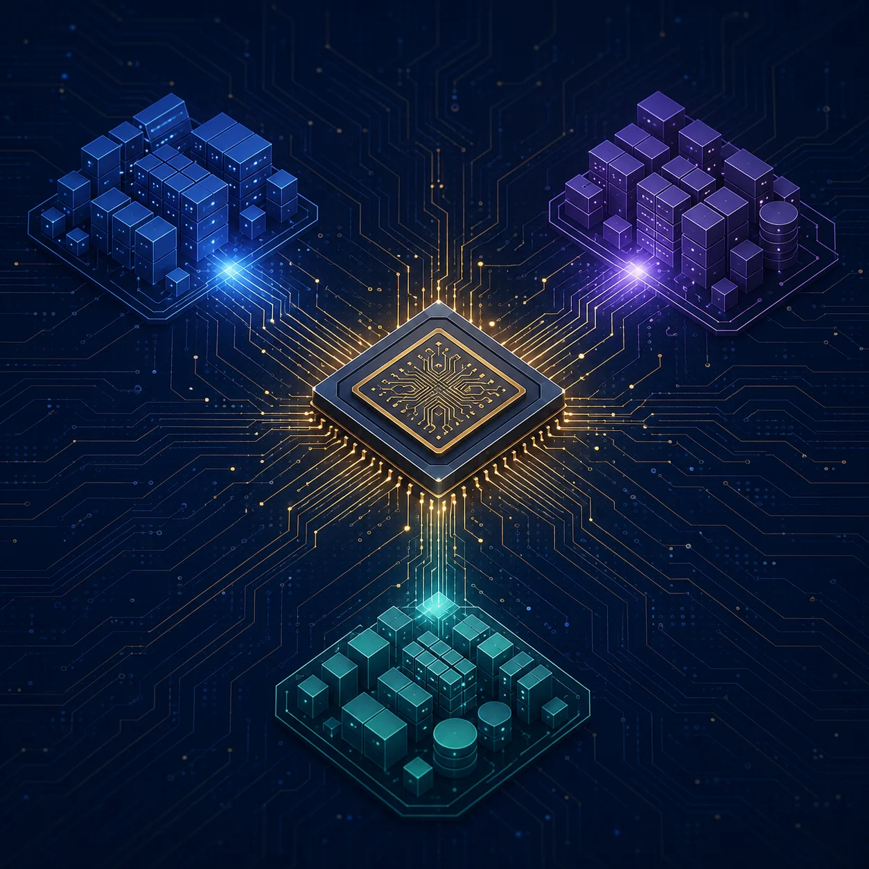
How XPUs and Networking Drive Broadcom’s AI Revenue Mix
Broadcom’s AI revenue is roughly split between two product categories. The first is the XPU chip design and production business — Broadcom designs the chip in partnership with the hyperscaler, manufactures it at TSMC using N3 or N2 process nodes, and earns revenue on chip sales. The second, and in some quarters the larger contributor, is AI networking silicon: the Tomahawk and Jericho ethernet switch chips that interconnect the accelerator clusters inside AI data centres.
AI training requires tight coordination among thousands of accelerators running in parallel; the interconnect between them must move data at rates that keep the accelerators fed without creating bottlenecks. Broadcom’s 51.2 Tbps Tomahawk 5 ethernet switch is the dominant switching silicon for high-bandwidth AI cluster interconnects, with deployments at every major hyperscaler’s AI data centre construction programme. Nvidia’s Blackwell infrastructure uses a mix of NVLink (Nvidia’s proprietary interconnect) for dense in-rack coupling and ethernet (often Broadcom Tomahawk-based) for rack-to-rack fabric — meaning Broadcom’s networking business benefits from Nvidia deployments as well as from custom XPU deployments that do not use Nvidia at all. The networking revenue is effectively a toll on all AI data centre construction regardless of which accelerator chip is inside.
Why Nvidia Hasn’t Lost and Why That May Change
Nvidia’s dominance in AI compute is not threatened by Broadcom’s XPU business in the near term, and the reason is timing and scope. Custom silicon development takes 3-4 years from design inception to volume production; the workload must be stable and large enough to justify the design investment; and the chip must be maintained and iterated in partnership with a single customer who accepts the risk of the design not performing as expected. These conditions apply to a small number of hyperscalers with the largest and most stable AI workloads. For the 99 percent of AI compute buyers who are not at Google or Meta scale — enterprises, cloud customers, AI startups, research teams — Nvidia’s general-purpose GPUs with their mature software ecosystem (CUDA, cuDNN, TensorRT) remain the only viable option.
The long-term dynamic is that custom silicon’s share of total AI compute will grow as more hyperscaler-scale workloads mature and as the design ecosystem improves. Hyperscaler cloud capex is increasingly allocated toward custom silicon as a percentage of total chip spend, and Amazon’s Trainium3 (a Broadcom-adjacent programme) and Microsoft’s Maia 2 represent additional major hyperscalers moving down the same path. Whether Broadcom retains the dominant position in XPU design-and-manufacture or faces competition from other chip design firms as the market grows is the strategic question for the post-2026 period; for now, its three-customer concentration in XPUs and its networking silicon monopoly position give it an AI revenue trajectory that no other semiconductor company outside Nvidia can match.
Broadcom’s XPU Position Is a Switching-Cost Moat Disguised as a Technology Advantage
The competitive analysis of Broadcom’s custom silicon business requires distinguishing between two different sources of durable advantage. The first — technology leadership, meaning a design capability that competitors cannot match — is valuable but perishable. A better chip design from a new entrant can erode technology leadership. The second — switching cost, meaning the accumulated cost to a customer of replacing the incumbent — is durable in proportion to how deeply embedded the incumbent’s knowledge is in the customer’s operations. Broadcom’s XPU position is the second type disguised as the first.
Custom silicon development for a hyperscaler takes 3-4 years from design inception to volume production. During that period, Broadcom’s engineers and Google’s ML infrastructure teams co-develop an architecture whose decisions — memory bandwidth ratios, precision formats, interconnect topology — reflect years of iterative learning about Google’s specific Gemini training and inference workloads. The resulting chip embodies knowledge that is not separable from the co-design relationship. Replacing Broadcom as Google’s XPU design partner would not be a procurement decision; it would be a 3-4 year re-design programme undertaken while Google’s most critical AI workloads run on a chip designed for a prior generation of models.
The switching cost compounds with each chip generation. By the time Google runs on TPU v6, the accumulated co-design knowledge from v4 and v5 is embedded in Broadcom’s team’s understanding of what Google needs. The TSMC manufacturing constraint adds a second-order lock-in: even if a hyperscaler wanted to change design partners, access to N2 process node capacity at the volumes required for a competitive custom chip is constrained independently of who designs it. The moat around Broadcom’s XPU business is therefore two layers deep — relationship switching cost at the design layer, and manufacturing access constraint at the production layer.
Michael Porter is the Bishop William Lawrence University Professor at Harvard Business School and the author of Competitive Strategy and Competitive Advantage. His Five Forces and value chain frameworks remain the dominant vocabulary for evaluating structural competitive positions.